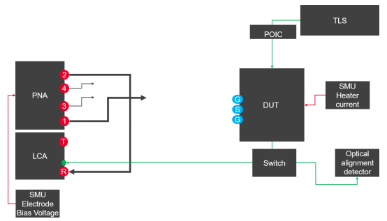
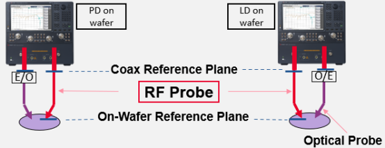
1. Advanced test hardware: industry-leading probe station and photoelectric test instrument, built-in automatic calibration program and instrument unembedding function, to ensure the accuracy, high precision and reliability of long-term test results.
2. Automatic test process: high degree of automation, reduce the need for manual operation, improve the consistency and repeatability of the test.
3. Customized software interface: Based on the powerful underlying driver and test logic library, the software interface can be customized according to the specific needs and operation habits of users to improve the convenience of user operation and the efficiency of the test process.
4. Flexible configuration: Multiple tunable laser sources can be configured to cover a wide range of test wavelengths. Coupled with the automatic optical probe coupling alignment system calibration can support a variety of multi-port passive optical chips (CWDM/DWDM optical multiplexer/demultiplexer /PLC optical splitter/array waveguide AWG chip) On-wafer level testing.
5. Easy to use graphical user interface: Provide intuitive user interface, simplify the test process, easy for users to get started, fast data analysis and test management.
6. Test data processing ability: powerful data processing function, support the storage of test results, analysis and report generation, facilitate long-term performance monitoring and quality assessment.
1. Support 4/8/12 inch wafer test;
2. The output wavelength of 1240-1380 nm/ 1340-1495 nm/ 1450-1650 nm/1490-1640 nm covers the OESCL measurement band; Maximum scanning speed 200 nm/s; Maximum power: > +12 dBm; Absolute wavelength accuracy: ±1.5 pm; Signal to SSE ratio: ≥ 80 dB/nm;
3. Fast switching of 6 SOP, up to 10μS; Provides stable output of 50μS;
4. Minimum sampling time 1μS;
5. Single channel optical coupling time ≤2S;
6. 0℃~125℃ environment test;
7. PA level direct basin test;
8. Test items include: wavelength domain /DC test, IL/PDL/ Responsivity/DC CMRR /PER /PD Dark current/ power /L-I-V curve/spectrum/wavelength, etc.
Frequency domain test: bandwidth, S parameter, delay, return loss, etc.


